Synchronous Serial Interface (SSI)
SSI stands for Synchronous Serial Interface and describes a digital synchronous interface with a differential clock line and a differential data line.
With the first falling clock edge, the data word to be output is buffered in the BTL to ensure data consistency. Data output takes place with the first rising clock edge, i.e. the BTL supplies a bit to the data line for each rising clock edge. In doing so, the line capacities and delays of drivers tv when querying the data bits must be taken into account in the controller.
The max. clock frequency fClk is dependent on the cable length (see Maximum SSI clock frequency depending on the cable length). The tm time, also called monoflop time, is started with the last falling edge and is output as the low level with the last rising edge. The data line remains at low until the tm time has elapsed. Afterwards, the BTL is ready again to receive the next clock package.
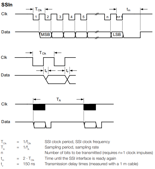
The BTL works in asynchronous operation. If the minimum sampling time is undercut, the BTL outputs the same position value several times. The external sampling rate is then greater than the internal rate. In addition, TA must be long enough so that the next clock package does not occur in the tm range of the previous package.
Data format
The BTL with SSI interface has the following factory settings:
Number of bits: 24, 25 or 26
Binary or Gray coded
Rising or falling

Example 24-bit SSI data frame with position data
M = MSB (Most Significant Bit)
L = LSB (Least Significant Bit)
The content of the information to be transmitted (e.g. position or velocity) is configurable. The MSB is always transmitted first.

Example of a complete data transmission (number of bits = 16)
Depending on configuration, position or velocity data may be signed. Negative values are output in two’s complement by default. For positive speeds, the position magnet moves away from the connection side; for negative speeds it moves toward the connection side. The controller must then be set to process signed data.
Depending the configuration, the device can output additional data following the main process data (e.g., 24-bit position and 8-bit temperature).
Example with 24 bit position data:
Additional data enable |
Main data |
Additional data |
Data bits (in total) |
|---|---|---|---|
Disabled (default) |
Position (24 bit) |
- |
24 |
Enabled |
Position (24 bit) |
Temperature (8 bit) |
24 + 8 = 32 |
Advanced settings
Besides factory settings following interface related parameters can be modified (see Comissioning):
Number of bits
Monoflop time tm
Coding (binary/Gray)
Additional error and parity bit (even or odd)
Multiple transmission mode
Output characteristic
Error value
Representation of negative values (two’s complement or sign bit mode)
Data resolution
Enable additional data output
Note
Error and parity bits are stuffed into the SSI data frame to the highest bit positions (MSB) by not extending the configured number of bits. Parity bit is always the MSB (if enabled).
Note
If additional data with Gray coding is enabled, Gray coding is applied separately to both data parts!
Faulty query
Underclocking
If there are too few clock edges, the current data level will be maintained for the time to (to = 2 x TClk timeout times) after the last negative edge from Clk. If, however, another positive edge occurs, the next bit will then be output. Afterwards a To event will occur, the data output goes to Low and after time tm has elapsed to High. The high level is maintained until the next clock burst. Time tm following to.
Overclocking
If there are too many clock edges, the data output will switch to low after the correct number of cycles has been completed. The tm timer is reset for every additional negative edge of Clk and internally the Tm event is set. After time tm the data again goes to high. A To or Tm event is shown in the status field as a communication error. In summary a communication error can have the following causes:
The bit number set in the BIR does not correspond to the bit number in the controller.
nBTL > nPLC → To event
nBTL < nPLC → Tm eventThe SSI clock frequency is too low
fClk < 9.771 kHz → To eventThe pause between two clock packages is too short → Tm event
Asynchronous operation
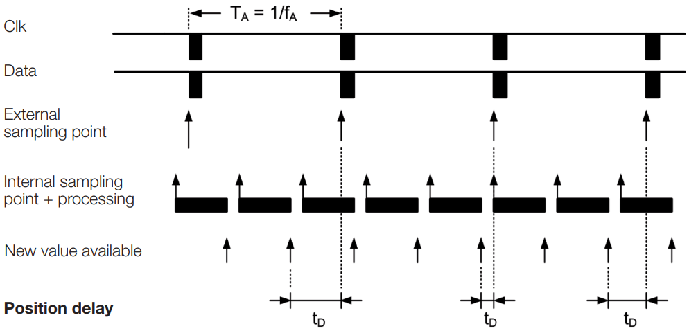
During asynchronous operation, the external sampling frequency is independent of the internal sampling frequency of the BTL. Depending on the external query point, the position is more or less current and the position delay tD is not constant. In the worst case, it is equal to the internal sampling period. The BTL always works with the maximum possible internal sampling frequency. Due to the measuring principle, the maximum sampling frequency fA,max is dependent on the nominal length of the BTL. The following graphic shows the behavior of internal and external sampling in asynchronous operation:
Note
The sampling frequency is the reciprocal value of the time between two clock packages and may not be confused with the SSI clock frequency.
Data multiplexer
The device has two special digital inputs labeled La and Lb (see Electrical Connection) which can be used as multiplexer inputs to select various pre-defined data formats for SSI.
Note
Changing the settings on these inputs affects only the output of additional data.
By default these inputs are inactive. For detailed information on the configuration options and on how to enable these inputs, see SSI output configuration.